Dielectric Withstanding Voltage (Hipot Method) – Thin Dielectric Layers for Printed Boards
1 Scope The dielectric withstanding voltage test (Hipot test) consists of the application of a voltage higher than the operating voltage for a specific time across the thickness of the test specimen’s dielectric layer. This is used to prove that a printed board can operate safely at its rated voltage and withꢀstand momentary voltage spikes due to switching, surges, and other similar phenomena. Although this test is similar to a voltage breakdown test, it is not intended for this test to cause insulation breakdown. Rather, it serves to determine whether the test specimen’s layers have adequate withstanding voltage. This document is applicable to thin dielectric materials such as those defined by IPC-4821. The results can be indicative of a change or a deviation from the normal material characteristics resulting from manufacturing, processing or aging conditions. The test is useful for quality acceptance and in the determination of the suitability of the material for a given application and may be adapted for process control.
2 Applicable Documents
IPC-4821Specification for Embedded Passive Device Capacitor Materials for Rigid and Multilayer Printed Boards
3 Test Specimen
3.1 Qualification Testing
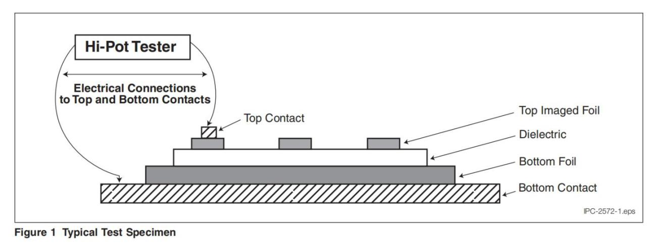
For laminate-like capacitor materials, test specimens shall be 50 mm [1.97 in] diameter circular electrodes (see ‘‘Top Imaged Foil’’ in Figure 1) that shall be formed by imaging and then etching the copper foil, unless otherwise as agreed upon by user and supplier (AABUS). Spacing between adjacent Top Imaged Foil conductors is recommended to be ≥100 times the dielectric thickness. In order to avoid field gradient and mechanical stress concentration, which can cause faulty dielectric breakdown, the Bottom Foil can be either a circle larger than the Top
Imaged Foil or can be a continuous copper sheet. The continuous copper sheet will be required for very thin capacitor dielectric layers that are not self-supporting. For nonlaminate-like capacitor materials, the test specimen’s Top Imaged Foil can be a size other than a 50 mm [1.97 in] diameter circle, if this size is not practical or typical. The test specimen’s Top Imaged Foil size for these nonlaminate-like materials should be set to the largest size normally recommended for this product (see 5.2.4). The thickness for the test specimens should be the typical/recommended thickness. A minimum of five test specimens shall be tested for qualification.
3.2 Conformance Testing
Test specimens can be the same as used for qualification testing or can be other sizes or shapes. For testing in printed board environments, actual innerlayer power and ground features are typically used, although other board features or test specimens can also be used. Please note that adjustments for capacitor plate size are required in the test procedure (see Section 6).
3.3 Test Specimen Conditioning
All qualification test specimens shall be conditioned at 23 °C ± 3 °C and 50% ± 10% RH for 24 hours, before testing. For conformance testing, such conditioning is optional.
4 Apparatus
4.1 Hipot Test Instrument
A Hipot test instrument is a piece of equipment capable of supplying a range of DC test voltages appropriate for the materials under test with adjustꢀable ramp rate and hold-time settings. The Hipot equipment shall have an adjustable threshold current setting. (see 5.2.4) The user shall ensure that the Hipot test instrument satisfies the original manufacturer’s technical specifications.
4.2 High Voltage Connections
Contacts (conductor plates) apply the voltage from the Hipot test instrument to the test specimen’s Top Imaged Foil and Bottom Foil (see Figure 1). These contacts should not contain sharp points that could damage either the copper foil or the dielectric layers of the test specimens. CAUTION: Dangerous voltages may be present on the test connections. Use proper
machine guarding and/or machine interlocking.
5 Procedure
5.1 This test method shall be performed on fresh test specimens. Hipot testing shall not be conducted on test specimens that have previously been exposed to high voltage levels or other similar testing. NOTE: Some dielectrics may show acceptable Hipot results (i.e., ‘‘Pass’’) after defects have been ‘‘burned out’’ at high voltage (see Section 6).
5.2 Program the Hipot test instrument with the appropriate peak voltage, voltage ramp rate, hold time at peak voltage and current threshold level. These values shall be recorded.
5.2.1 The peak voltage should be as specified in the mateꢀrial Specification Sheet (see IPC- 4821) under the parameter ‘‘Hipot (Volts DC).’’
5.2.2 For qualification testing, the voltage ramp rate shall be 5% of the peak voltage per second, unless otherwise specified. For conformance testing, the voltage ramp rate shall be 5% of the peak voltage per second or AABUS.
5.2.3 For qualification testing, the hold time at peak voltage shall be 30 seconds +3 / -0 seconds. For conformance testꢀing, the hold time at peak voltage shall be a minimum of 10 seconds or AABUS.
5.2.4 The threshold settings shall be set to a value greater than the in-rush current (due to the charging of the test speciꢀmen) observed when the voltage is increased (see 6.1). Many commercial Hipot test instruments display the current during the test. The in-rush current can be determined by setting the threshold current to a high value and then observing the curꢀrent spikes as the voltage is ramped to the peak voltage. After several test specimens have been tested and the currents observed, set the threshold current to be greater than the highest current observed. For example, if the in-rush current is 20 microamperes and the current at peak voltage is 1 microꢀampere, set the threshold current to 40 microamperes.
5.3 The test specimen shall be placed between the conꢀtacts of the Hipot test equipment (see Figure 1). Start the Hipot sequence.
5.4 Upon completion of the test, the Hipot sequence should include the discharge of the test specimen. SAFETY NOTE: Larger test specimens, with high capaciꢀtance density, may take more time than expected to disꢀcharge.
5.5 Reporting The Hipot test instrument indicates either Pass or Fail of the material under test. A current surge above the threshold current setting indicates a Failure. This includes very short term current surges or ‘‘arcs’’ that occur due to the burnout of defects. Such unacceptable current surges may also be the result of dielectric failure or manufacturing defects. For qualification testing, if the test specimen Passes, record the leakage current per unit area and the passing voltage. If the qualification test specimen Fails, record the failure voltage and threshold current per unit area of each test specimen. For conformance testing, reporting requirements should be AABUS.
6 Notes
6.1 When the Hipot test instrument voltage changes from one level to the next higher level during the ramp-up to the final voltage, the in-rush current will initially surge above the steady state current because the capacitor is charging. It is possible that this surge in current could exceed the thresholdcurrent preset on the Hipot test instrument, causing the instrument to indicate a failure when in fact there was none. The charging current of the capacitor is affected by the change in voltage from one ramp step to another, the dielecꢀtric constant of the dielectric, the thickness of the dielectric and the area of the capacitor. High dielectric constant, very thin dielectric thickness and large area of the capacitor plates will all cause the charging current to increase. As a result, the threshold current setting on the Hipot test instrument may need to be adjusted to avoid generating a false failure condition.
6.2 Some thin and filled dielectrics will require a higher threshold current setting, compared to unfilled materials. This is particularly true of dielectrics containing ferroelectric comꢀpounds, such as barium titanate. These materials may show a nonlinear response between current and voltage. This is not an issue at most operating voltages, which are normally low, but can be an issue for the Hipot test. At high voltage levels, these materials may trigger a false failure because they allow more current than the threshold setting.
6.3 Materials, especially very thin and/or highly filled materials, may have a leakage current per unit area that is area dependent when tested at the specified test voltage. Thus, results from the qualification test specimen or other small area test structures may not reflect the actual leakage current per unit area when the material is tested in asignificantly larger area format, such as that commonly done in conformance testing by a material supplier.
6.4 Reference Documents ASTM D149 ‘‘Dielectric Breakdown Voltage of Solid Electrical Insulating Materials at Commercial Power Frequencies’’